


|
PCB Design |
|
CAD Tools
· Pads Power SCH · Pads Power PCB · Orcad Schematic · Allegro PCB · Protel · Altium · Solid Works · Gerber Editor/Viewer · CAM350
|

|
PCB Design |


|
(619) 721-0402 |
|
Capabilities
· Single layer · Double layer · Multilayer · High Speed · Impedance controlled · RF · Ground/Power planes · Thru-hole & SMT · Mixed technology
|
|
Services
· Schematic entry · Layout design · Gerber file generation · Engineering changes · Reverse engineering · Cost reductions · Validation & Verification · Quick turn prototyping · Low volume runs
|
|
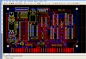
PCB DESIGN SERVICES Schematic entry, PCB layout design, Gerber files and Manufacturing drawings are at the heart of the electronic design process. We develop them with strict compliance to EMC, ESD, IPC and Safety design standards using the latest electronic design, simulation and modeling CAD tools.
PCB DESIGN PROCESS EXPLAINED
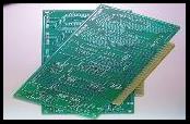
A PCB or Printed Circuit Board mechanically supports and electrically connects electronic components using conductive traces. It is also known as Printed Wiring Board and when populated with components it is known as PCBA or Printed Circuit Board Assembly.
The PCB Design process normally involves the next steps:
· Schematic capture · Component footprint development · Mechanical planning · Technology determination · Layers stack up planning · Line impedance planning · Component placement · Routing · Design rule checks · Final Preparation (silkscreen, finish, etc.) · Manufacturing files generation
SCHEMATIC CAPTURE ……….more on Schematic Capture Schematic capture is a step in the PCB Design process. Here the electronic diagram is developed by a designer and entered into a CAD system.
Cad tools There are plenty of options in the process of selecting the CAD tool. The PCB designer can choose from simple low-end, free or low cost to highly sophisticated and expensive options. The typical tools include: Eagle, P-Cad, Orcad, Allegro and Altium among others.
Component Creation Once the CAD tool has been selected, the PCB designer needs to create components. This include from low-end components like resistor or capacitors to high-end, high-pin-count integrated circuits. The component is represented by a graphical symbol with pins attached to it. The pins actively represent inputs, outputs, load and power. Additional component properties like footprint, part number and description are assigned to the symbol.
Component Libraries The components are organized in libraries. The library can have sections for filing different component categories. Some CAD tools include a basic library of components. The libraries can be local to the computer where the CAD tool is installed or remotely accessible via servers.
Schematic Workspace Page Set-up Before placing components the new PCB design workspace needs to be set-up. This include selection of page size, visual grids, design grids, wire width and design elements colors among others.
Components Placement Component placement is the act of moving components from the libraries to the workspace. Sometimes it is possible to copy components from one schematic page to another or from one design file to another. Every component is identified by a unique reference designator.
Wiring Up In order to interconnect components, wires (nets) are traced between component pins. The wires can be a single line connection or a bus representing multiple lines connection. The graphical distribution of the wires must avoid confusions in the visual interpretation of the connections (e.g. avoid 4-way ties). One way to minimize the visual density of the interconnect wires in complex, dense designs is to make use the multiple pages to separate different functional design blocks. The different schematic pages can now be connected using off-page connectors which are virtual wires running from one page to another. In addition to off page connectors there are in-page connectors which help to minimize the graphical density of intra page wires.
Schematic Design Elements The next are the typical schematic design elements: Component symbols, reference designators, nets, buses, net names, power and ground symbols, off-page connector, on-page connector, dots (unions), title block and text (notes).
Schematic Design Rule Check In order to verify the correctness of the design, design rule checks must be run on the CAD tool. This process identifies issues like short circuits, duplicate ref designator, single ended nets or pin input-output conflicts. The successful completion of this step is needed before generating the final schematic output (netlist).
Netlist Generation Once the design has passed the rule checks, the designer can go ahead and generate the final schematic output which is named “Netlist”. The netlist is a coded representation of all the connections between all the component pins in your design. The netlist can include additional information (e.g. component footprint assignation, current handling capabilities, maximum length, etc.).
PCB FOOTPRINT DEVELOPMENT Footprint development is another step in the PCB Design process. Here the component land pattern is developed by a designer using a CAD system. The land pattern is the copper etched surface where the component pins have mechanical contact with the PCB. The typical elements of a footprint are:
PADS This is the individual copper etched surface geometry where the component pin comes in contact with the PCB or it’s inner layers equivalent. The total pad stack-up depends of the number of layers and if the footprint is for a thru-hole or surface mount component. The typical pad elements are shape, width, length, orientation, drill size, plating and pin number.
KEEP-OUTS OR KEEP-IN Keep-out or keep-in are geometrical boundaries which defines design constrains like component outline, proximity limits and placement limits.
TEXT Text is used to add visual description of some footprint attributes like component name, type, footprint name and pad number among others.
ORIGIN All the footprint design elements are referenced to the footprint geometrical origin. It can be pin 1 or the geometrical center of the footprint. The origin position has design implications on placement, movement, aligning and dragging of the footprint during the PCB design process.
PCB MECHANICAL PLANNING Several mechanical design decisions must be accomplished before placing components on the PCB design workspace. Every PCB eventually will be mechanically installed. These are the typical PCB mechanical planning areas:
PCB Outline The outline defines the overall board dimensions and shape. It must be planned considering all the possible mechanical constrains. Sometimes the outline has standardized dimensions in order to be compliant to board form factors like PC104 or VME. Additionally, electrical constrains like high voltage isolation or noise immunity affect the board outline shape and dimensions.
Connectors position One of the key mechanical considerations in the PCB design process is the position of connectors. The connectors provide the board connectivity for several functions like programming, communication, expansion, backplane interconnection, user interfacing, front panel interconnections and more. So the position of connectors in the PCB surface is highly related to its function.
Component height vs. position The final PCB assembly at some point will be installed in some sort of mounting structure. This PCBA sub-assembly will be in close proximity to other sub-assemblies. So component height and position planning is key to avoid mechanical and electrical issues like interference, noise induction, heat induction and others.
PCB Mounting Holes The PCB mounting holes are critical to the successful mechanical performance of the printed circuit board. They establish the overall position and mechanical support of the PCB assembly in relationship to other system elements. The mounting hole pad diameter and drill size must be carefully selected according to the fastening element to be used like screws, inserts or rivets. Additionally, the distance to other components should be considered. The mounting hole can be electrically isolated or connected to ground. If the mounting hole is isolated, it is preferable to avoid the plating of the thru-hole because of the possible metallic residues coming from inserting erroneously selected screws which can short circuit components. Sometimes the mounting hole-screw assembly can be used as heat sink.
PCB TECHNOLOGY DETERMINATION The PCB technology refers to the overall electrical and mechanical sophistication of the printed circuit board. Initially determined for the minimum trace width, trace separation, pad / via diameter and drill size. The cost of the printed circuit board is directly proportional to the selected technology level. The higher the technology, the higher the cost.
PCB Material The final printed circuit board is in reality a stack of different layers including conductive, insulation and finish. The conducting layers are made of copper foil and can be selected in several copper densities. The insulation layers are made of several materials in order to provide different dielectric constants according to the various circuit requirements. The typical materials are FR-4 (woven glass and epoxy), FR-6 (mate glass and polyester), CEM-1 (Cotton paper and epoxy) and CEM-3 (woven glass and epoxy). The most common material is FR-4.
PCB Trace Width The minimum trace width of a PCB must be selected according to factors like minimum current handling needs, trace impedance, available manufacturing process and cost. The typical minimum trace widths range from 4 to 8 mils.
PCB Trace Separation The minimum trace separation of a PCB must be selected according to factors like maximum working voltage, trace impedance, available manufacturing process and cost. The typical minimum trace separations range from 4 to 8 mils.
PCB Pad and Via Diameter The minimum pad /via diameter of a PCB must be selected according to factors like minimum current handling needs, pad inductance, available manufacturing process and cost. The typical minimum pad / via diameters range from 20 to 30 mils.
Drill Size The minimum drill size must be selected according to factors like minimum current handling needs, pad / via inductance, available manufacturing process and cost. The typical minimum drill size range from 10 to 15 mils.
PCB LAYERS STACK-UP PLANNING The PCB layer stack-up planning is a key part of the PCB design process. It has determinant effects on signal integrity, trace density and EMC footprint.
The minimum factors to select are: · Number of layers · Number of planes · Order of layers · Spacing between layers
The key conditions to achieve are: · Signal layers must be routed adjacent to planes · Power and ground planes must be close coupled (adjacent). · High-speed signals must be routed in layers buried between planes. · The use of multiple ground planes.
PCB LINE IMPEDANCE PLANNING The line impedance planning has strong effects on signal integrity. The trace width and separation must be calculated according to the different line impedances needed (e.g. 50Ω, 90Ω, 100Ω, etc.) for single ended and differential lines.
PCB COMPONENT PLACEMENT Component placement is another of the key steps in the PCB design process. It is critical to the final performance of the board. It involves the use of grids, grouping of components according to function, keep outs, thermal and manufacturing considerations among others.
Placement guidelines:
Grids The placement must be accomplished using defined design grids in order to provide a geometrically stable positioning for Pick & Place and In Circuit Testing purposes.
Functional blocks Component blocks must be formed according to functional conditions. There are several levels of partitioning the design like top level in analog, digital and power. Lower level partitions must be developed for each functional block. In general the partitioning in blocks must consider signal integrity, EMC, ESD, power demands, keep-outs, thermal footprint, induction, crosstalk and accessibility for testing and manufacturing.
Component Orientation Never forget that critical working parameters and conditions like signal integrity, EMC, ESD, power demands, keep-outs, thermal footprint, induction, crosstalk and accessibility for testing and manufacturing always take precedence over nicely lined-up components. But whenever possible, the components must be lined up in order to facilitate manufacturing, testing and service. In general terms, the ICs should face the same direction, resistors organized in rows / columns, the blocks of polarized components (capacitors, diodes, etc.) should have the same orientation and the connectors should be placed at the edge of the board.
PCB ROUTING Routing is the action of laying out the traces from pin to pin according to the Netlist. Once again, the routing must be accomplished considering signal integrity, EMC, ESD, power demands, keep-outs, thermal footprint, induction and crosstalk among others. The basic routing elements are traces, vias, planes and footprints.
Traces The traces are one of the four basic routing elements. The forming elements of the traces are width, length, separation to other traces or electrical shapes, trace angle and pad connection. As you can imagine, these elements have major implications on signal integrity, current handling capabilities, resistance, inductance, capacitance, noise coupling, reliability, manufacturability and cost.
Planes The planes are copper surfaces electrically connected to power and ground nets. In one single layer you can have one complete plane or several split planes. Split planes normally apply to power planes because it is highly desirable not to have split ground planes due to signal integrity issues. Again, these elements have major implications on signal integrity, current handling capabilities, resistance, inductance, capacitance, noise coupling, reliability, manufacturability and cost.
Vias The vias are the forgotten routing element. Normally, we use them but don’t pay so much attention to their impact in the design. Their quantity, position, diameter and drill size are determinant in the correct performance of the PCB design. Again, these elements have major implications on signal integrity, current handling capabilities, resistance, inductance, capacitance, noise coupling, reliability, manufacturability and cost.
Footprints The conditions of the point of contact between the traces and the pads of footprints are critical for the correct performance of the PCB design. It has implications on manufacturability, thermal handling and signal integrity.
PCB Routing Guidelines · Make the trace width according to current demand needs. · Make the trace width according to line impedance requirements. · Make the trace width according to manufacturability constrains. · Keep the trace length as short as possible to reduce resistance, capacitance and inductance. · Keep the trace length as short as possible to reduce noise and crosstalk. · Keep the proper separation between high speed and low sped traces. · Keep proper clearance for high voltage circuits. · Route power critical traces and high speed lines like clocks and differential pairs at the beginning. · Route high speed traces in layers buried between ground planes. · Avoid tracing lines at angles higher than 45 degrees. · Finish the traces on the center of the pads. · Make use of thermal reliefs as required. · Make use of the power, ground and signal layers. · Minimize the number of vias. · Use multiple vias for high current traces. · Provide test points for each net.
PCB DESIGN RULE CHECKS It is important to perform PCB layout design checks before generating the final documentation. Normally, the PCB design CAD tool has automatic modules to conduct this check. The basic items to be checked are:
· Connectivity according to netlist information. · Clearances between routing elements like traces, vias, planes and components. · Routing rules like trace length and width. · High speed rules like Trace length, match length, parallelism, impedance, delay, capacitance and stub length. · Pad entry and fan out.
PCB FINAL PREPARATION Once all the above steps are complete the PCB design needs to go through the final preparation process. Here items like silkscreen, soldermask and finish are refined. The silkscreen trace width should be set according to the manufacturing process to be legible, the soldermask color selected and the exposed copper surface finish determined.
PCB MANUFACTURING FILES GENERATION The last step in the PCB design process is the manufacturing files generation. This is a collection of electronic files containing all the needed information for manufacturing the newly designed PCB. The next are the typical files:
· Manufacturing drawing with board dimensions, layers stack-up and notes. · Gerber files in format RS-274X. · Drill drawing. · Drill file in NC format.
Gerber Files A Gerber File is a file format to transfer artwork information to PCB manufacturing machines. The gerber files also contain drilling and dimensional information. The original gerber file standard RS-274D represents the artwork information of each layer in two separate files. The new RS-274X represents the artwork information in a single file.
The basic gerber files are:
.GTL Top Layer .GBL Bottom Layer .GTS Top layer soldermask .GBS Bottom layer soldermask .GTO Top layer silkscreen .GBO Bottom layer silkscreen .GTP Top layer solder paste .GBP Bottom layer solder paste .GM1 Mechanical layer #1 .GDD Drill drawing
Additional files can be included if inner layers are present..
|
|
Copyright - Echazarreta Systems - 2019 |