|
Schematic Capture |
|
(619) 721-0402 |


|
SCHEMATIC CAPTURE Schematic capture is a step in the PCB Design process. Here the electronic diagram is developed by a designer and entered into a CAD system.
SCHEMATIC CAPTURE PROCESS EXPLAINED
· CAD tools · Components · Component Libraries · Global Set-up · Projects · Design preferences · Schematic page editor · Design Elements · Placement · Wiring · Rule checks · Final output
Schematic CAD Tools
CAD Defined Computer-aided-design (CAD) is the use of computer technologies to facilitate the design process. CAD tools are at the center of the schematic capture. They provide the user with a rich set of resources and features to simplify and standardize the design process. CAD tools may include 2D modeling, 3D modeling and functional simulation.
Schematic CAD Tool Options There are plenty of options in the process of selecting the schematic CAD tool. The PCB designer can choose from simple low-end, free or low cost to highly sophisticated and expensive options. The typical tools include names like:
- Eagle - P-Cad - Orcad - Allegro - Altium
Schematic CAD tool Features and Capabilities CAD tools offer numerous features that facilitate the Schematic entry process. The typical features are:
- User friendly intuitive environment - Project manager interface - Component editor - Library manager interface - Schematic editor - PCB design flow integration - Schematic design verification interface - Functional simulation
Schematic CAD Benefits The user friendly and intuitive environment accelerates the learning and using of all the features in the CAD tool. It boosts efficiency in schematic editing for fast capture of the design details.
The project manager interface keeps all the project elements well organized for easy access and use. It normally represents all the elements in a tree format. In this way you can see all the dependencies and interactions among all the project elements in a single view.
The component editor facilitates the creation of new components. You can develop a new component from scratch or you can edit an existing component and save it with a different name. Schematic CAD tools normally provide access to manipulate the schematic component design elements.
The library manager interface facilitates the manipulation of component libraries. You can add or delete components or you can copy components from one library to other. Libraries may be specialized per component type, per component manufacturer or any other combination.
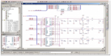
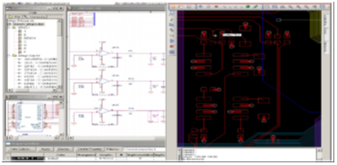
The schematic editor is the key interface of this CAD tool. This is the interface that makes active use of the most of CAD features. The flat and hierarchical schematic page capabilities facilitate the design connectivity. It makes easy to handle from simple single page designs to complex multi-page projects.
Schematic Components Components are the basic building blocks of the schematic. They include from low-end parts like resistor or capacitors to high-end, high-pin-count integrated circuits. Components are represented by a graphical symbol with pins attached to it. The pins actively represent inputs, outputs, load and power. Additional component properties like footprint, part number and description are assigned to the symbol.
Schematic Component Graphics Schematic component symbols at the CAD level are made of outlines and graphics. The outline reflects the component shape and follows the grid set up. Inside the outline, you can draw graphics to add detail to the component symbol. To add graphics to the component, you can use lines, rectangles, ellipses, arcs, polylines and pictures. Additionally, you can add text and/or IEEE graphics to the symbols.
Schematic Component Pins Pins are the electrically active elements of the component symbols. They are an essential part of the connectivity system and are referenced at the final schematic capture netlist output level. The basic pin properties are:
- Type - Name - Number
Pin types include options like 3 state, input, output, bidirectional, passive, power and open collector. The pin-type to pin-type connectivity can be verified at the “Design Rule check” level. Pin names are normally shown inside the component outline. Pin numbers are shown outside the component outline.
Schematic Component Properties Component properties are additional information, which further define the component. The typical schematic component properties are:
- Symbol name - Reference designator letter - Source library - Footprint name - Value - Description - Manufacturer - Manufacturer part number
Schematic Libraries Libraries are files that contain a collection of reusable components. They contain parts that you can place on your schematic. Libraries contain additional elements like power symbols, ground symbols and title blocks that you can reuse in your schematic projects. Some CAD tools include a basic library of components. The libraries can be local to the computer where the CAD tool is installed or remotely accessible via servers.
Standard & Custom Schematic Component Libraries Some CAD tools include a basic standard library of components. Or you can create custom libraries to keep any combination of items. Additionally, you can get or setup specialized libraries per component manufacturer or component category.
Create and/or Copy Schematic Component Libraries Libraries can be manipulated as normal files. You can create, delete, copy, archive and edit the whole library. Just remember that these actions apply to all the collection of items stored in the library.
Editing Schematic Component Libraries Inside a library, you can create, delete, copy and, save individual components. Or you can move components from one library to another.
Schematic Design Cache Normally, there is no need to create a library for a project. The project design cache stores all the components used in the project design.
Schematic Interface Global setup Schematic CAD tools allows you to setup global preferences for the schematic capture interface. The options that you define here, affect how to work with your projects. The typical schematic global setup preferences are: - Colors - Grid display - Pan & zoom - Select - Text editor - Miscellaneous
Schematic Projects A schematic project is a collection of design elements that belong to a single design. Projects store design elements like schematic folders, libraries, output files (netlist), and reports (design rule checks). A project can have one or more schematic folders. Each folder can have one or more schematic pages. The project also contain a design cache which stores a copy of all the components and symbols used on the schematics. Schematic CAD tools normally have a project manager interface that keeps all the project elements well organized for easy access and use. It normally represents all the elements in a tree format. In this way you can see the hierarchy, dependencies and interactions among all the project elements in a single view.
Schematic Design Preferences Before placing components, the new drawing preferences need to be set-up. This include the selection of preferences like fonts, title block information, page size, grids, Hierarchy, and compatibility.
Schematic Page Editor The schematic page editor is an interface that allows you to display and edit schematic pages. On the schematic page you can place components, wires, buses, text, and graphics. The schematic page editor normally includes menus like file, edit, view, tools, place, options, and window. Additionally, includes tools bars for placing and editing schematic objects.
Schematic Design Elements The typical schematic design elements are: Components, buses, nets, power / ground symbols, off-page connector, on-page connector, dots (unions), title block and text (notes).
Schematic Components Components are the basic building blocks of the schematic. They include from low-end parts like resistor or capacitors to high-end, high-pin-count integrated circuits. Components are represented by a graphical symbol with pins attached to it. The pins actively represent inputs, outputs, load and power. Additional component properties like footprint, part number and description are assigned to the symbol.
Schematic Nets Nets are the interconnect components of the schematic. Nets are traced between component pins. The net can be a single line connection or a bus representing multiple lines connection. The graphical distribution of the nets must avoid confusions in the visual interpretation of the connections (e.g. avoid 4-way ties). One way to minimize the visual density of the interconnect nets in complex, dense designs is to make use the multiple pages to separate different functional design blocks. The different schematic pages can now be connected using off-page connectors which are virtual wires running from one page to another. In addition to off page connectors there are in-page connectors which help to minimize the graphical density of intra page nets.
Schematic Buses Buses are a group of multiple nets represented for a single thick wire. The bus can be named in a scalar way, for example A[0:3]. This represents a four nets bus that connects four signals. If we continue considering the bus name A[0:3], the individual net names would be A0, A1,A2, and A3.
Schematic Power Symbols Power symbols are global connectors. The typical power symbols are +V and Ground. Multiple positive and negative (ground) power symbols can be used in the same design. But different net names must be assigned in order to differentiate from each other.
Schematic Off-page Connectors Off-page connectors provide connectivity between different schematic pages. Off-page connectors are connected by name to other off-page connectors within the same schematic.
Schematic Net Unions (dots) Net unions are graphical and electrical connections normally represented by dots. If two wires are crossing but the net union (dot) is not present, they are not electrically connected. If two wires are crossing and the dot is present, they are electrically connected.
Schematic Title Block The Title block is a special area of the schematic dedicated to describe general information of the new design like name, project, document number, document title, creation date, and revision.
Schematic Text Text entries can be included on any part of the schematic document. You can use different fonts, font sizes and any of the normal text effects like underlined, italic, and bold among others. Additionally, the text can be edited using the standard methods like copy, paste, cut, delete, move, and rotate.
Schematic Graphics Graphics can be added to the schematic page. Normally, the schematic page editor includes a toolbar to control graphics on the schematic page. The typical graphics are lines, rectangles, squares, circles, ellipses, arcs, polylines, and polygons. The graphic shapes can be rotated, moved, cut, copied, and deleted.
Schematic Placement Component placement is the act of moving components from the libraries to the workspace. Sometimes it is possible to copy components from one schematic page to another or from one design file to another. Every component is identified by a unique reference designator. It is a best practice to place components on the schematic page following the flow of the design and normally from left to right and from top to bottom. Sometimes the best approach is to complete the placement of component on the schematic page by grouping parts by function. If the design is complex, it is possible to group functional blocks by page and have multiple pages.
Schematic Wiring In order to interconnect components, wires (nets) are traced between component pins. The wires can be a single line connection or a bus representing multiple lines connection. The graphical distribution of the wires must avoid confusions in the visual interpretation of the connections (e.g. avoid 4-way ties). One way to minimize the visual density of the interconnect wires in complex, dense designs is to make use the multiple pages to separate different functional design blocks. The different schematic pages can now be connected using off-page connectors which are virtual wires running from one page to another. In addition to off page connectors there are in-page connectors which help to minimize the graphical density of intra page wires.
Schematic Design Rule Check In order to verify the correctness of the design, design rule checks must be run on the CAD tool. This process identifies issues like short circuits, duplicate ref designator, single ended nets or pin input-output conflicts. The successful completion of this step is needed before generating the final schematic output (netlist).
Schematic Final Output Once the design has passed the rule checks, the designer can go ahead and generate the final schematic output which is named “Netlist”. The netlist is a coded representation of all the connections between all the component pins in your design. The netlist can include additional information (e.g. component footprint assignation, current handling capabilities, maximum length, etc.). |
|
Copyright - Echazarreta Systems - 2019 |